Description
Kintex® UltraScale™ devices provide the best price/performance/watt at 20nm and include the highest signal processing bandwidth in a mid-range device, next- generation transceivers, and low-cost packaging for an optimum blend of capability and cost-effectiveness.Source: https://www.xilinx.com/products/silicon-devices/fpga/kintex-ultrascale.html
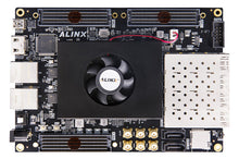
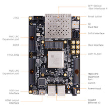
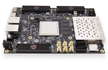
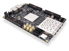
AXKU040 is our Best Selling KU Family Development Board, with XCKU040 FPGA in the centre, surrounded by abundant I/Os and Expansion Ports, easy access to unlimited performance for your Industry applications. With a size smaller than the A5 Work Diary, it has 4x 10G SFP+, 1x HPC + 2x LPC FMC, 6x SMA, and 2x SATA. A great compact dev board for fast-paced prototyping of high demanding projects.
Ideal for:
- Packet Processing in networking and data center applications
- DSP-intensive processing in next-generation medical imaging
- 8k/4k Video
- Heterogeneous wireless infrastructure
For a PCI Express form, check out our AXKU041 or AXKU042. For a SOM form, look at our ACKU040 or ACKU060.
Note: AXKU040 is a single PCB design, not a SOM + Carrier Board.Comparison
| FPGA | XCKU040-2FFVA1156I |
| Chip Level | Industrial Grade |
| Speed Grade | -2 |
| Logic Cells | 530K |
| CLB Look Up Tables (LUTs) | 242,400 |
| CLB Flip-Flops | 484,800 |
| Max. Distributed RAM (Kb) | 7,050 |
| Block RAM Blocks (36Kb each) |
600 |
| Total Block RAM | 21.1 Mb |
| Global Clock | 10 |
| I/O DLL | 40 |
| DSP Slices | 1,920 |
| PCIE Gen3 x8 | 3x |
| GTH Transceiver | 20x, 16.3 Gb/s max |
Features
| DDR4 | 4x 1GB DDR4, total 4GB, 64bit Bus, Data Rate 2400Mbps |
| QSPI FLASH | 1x 128Mbit, for user data storage |
| FMC Expansion Port | 3x Standard FMC Expansion Ports: 2x LPC and 1x HPC, for Xilinx/ALINX or 3rd Party FMC cards |
| HDMI Output | Support 1080p@60Hz, 3D Output |
| SFP+ | 4x SFP+ Interfaces, speed of each channel up to 12.5Gb/s |
| Ethernet Interface | 2x 10/100/1000M Ethernet with RJ45 for data exchange |
| SMA Interface | 6x SMA Interfaces, connecting external high speed signal |
| SATA | 2x SATA interfaces for external Hard Disk |
| JTAG | 10-pin 2.54mm (0.1-inch) Standard JTAG port for Programs Debug and Download |
| Temperature Sensor | LM75, for onboard ambient temperature |
| EEPROM | EEPROM 24LC04 with IIC |
| USB UART | for serial communication with PC or devices |
| Crystal Oscillator | 1x 200MHz for the FPGA; 1x 125MHz Clock Source for the SFP+; 1x 156.25MHz Clock Source for the GTH transceiver |
| LEDs | 1 Power Indicator, 1 DONE, 4x User |
| Push-Buttons | 1x Power Switch, 1x Reset, 2x User |
| SD Card Slot | 1x micro-SD Card Slot, support SD mode and SPI mode |
Power Supply
Voltage Input: +12 V DC, 2.1mm x 5.5mm
Current Input: Max. Current 3A
What's Included
| FPGA Board | 1 | DC Fan (installed) | 1 |
| Mini-USB Cable | 1 | Programming Cable | 1 Set |
| 12V Power Adapter | 1 | Acrylic Panel | 1 |
Dimensions
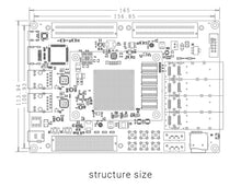
| Dimension | 165mm x 113.94mm |
| PCB | 14 Layer, with Independent GND and VCC Layers |


