Description
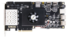
AX7Z035 is a Highly Versatile Mid Range Xilinx Zynq-7000 XC7Z035 PCI Express 2.0 Development Card with 4x SFP+, 2x SATA, 2x Gigabit Ethernet, 2x HDMI, 1x MIPI and PCIE x8, enabling highly differentiated designs for a wide range of embedded applications including ADAS, Medical Endoscope, Small Cell Baseband, Machine Vision and Multi-function Printers.
The SOM model used is AC7Z035.
The AX7Z100 shares the same carrier board with AX7Z035.
AX7Z035 is a SOM + Carrier Board design. For a single board design with PCIE Slot (ROOT MODE) check our AX7350.
FPGA Specification
| FPGA | XC7Z035-2FFG676I |
| Processor Core | Dual-Core ARM Cortex-A9 MPCore Up to 800MHz |
| Speed Grade | -2 |
| Chip Level | Industrial Grade |
| Working Temperature | -40℃~85℃ |
| Logic Cells | 275K |
| Look-Up Tables (LUTs) | 171,900 |
| Flip-Flops | 343,800 |
| Total Block RAM | 17.6Mb |
| (# 36Kb Blocks) | (500) |
| DSP Slices | 900 |
| PCI Express® | Gen2 x8 |
| Analog Mixed Signal (AMS) / XADC | 2x 12 bit, MSPS ADCs with up to 17 Differential Inputs |
| GTX Transceivers | 8x 12.5Gb/s |
| PS MIO | 128 (FPGA pin) |
| HR IO | 100 (FPGA pin) |
| HP IO | 150 (FPGA pin) |
Board Features
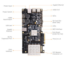
| DDR3 | PS: 2 Pieces of 512MB DDR3, 1GB total, 32 bit bus width, max rate 1066Mbps; PL: 2 Pieces of 512MB DDR3, 1GB total, 32 bit bus width, max rate 1600Mbps. |
| QSPI Flash | 2 Pieces of 256Mbit, for FPGA bin file and user data storage |
| eMMC | 8GB, for Large capacity storage in the ZYNQ system |
| PCI Express 2.0 | x8 connector, x4 lane, up to 5G Baud each lane. |
| SFP+ | 4x SFP+, up to 10.3125Gb/s each channel. |
| SATA | 2x SATA, for external HD Storage. (Not connected.) |
| Gigabit Ethernet | 2x 10/100/1000M Ethernet with RJ-45 |
| JTAG | 10-pin 2.54mm (0.1-inch) Standard JTAG port for Programs Debug and Download |
| HDMI | 1x Output, 1x Input, max 1080p@60Hz, supports 3D. |
| MIPI | 1x MIPI, for camera e.g. ALINX OV5640 |
| USB 2.0 | 4x USB 2.0, for USB peripherals |
| USB UART | for Serial Communication with PC/Devices |
| Crystal Oscillator | 33.333MHz Active to the PS, 200MHz Differential to PL DDR, 125MHz Differential to the GTX Transceivers. |
| 40-pin Expansion Port | 1x 40-pin Expansion Port (2.54mm / 0.1 inch pitch), fit with ALINX Binocular Camera Module, TFT LCD Screen, Camera, AD/DA, etc. Includes: 1x 5V, 2x 3.3V, 3x GND, 34x I/O. |
| Temperature Sensor | LM75, for onboard ambient temperature |
| SD Card Slot | 1 micro SD Card Slot, support SD Mode and SPI Mode |
| LED | SOM: 1 PWR, 1 DONE Carrier: 1 PWR, 1 DONE, 4 PL User, 2 Serial (TX/RX) |
| Push-Buttons | 1 Power, 1 Reset, 4 PL User |
Power Supply
Voltage Input: +12 V DC, Barrel plug 2.1 x 5.5mm
Current Input: Max. Current 3 A
What's Included
| FPGA Board | 1 | DC Fan | 1 (installed) |
| Mini USB Cable | 1 | Programming Cable | 1 set |
| 12V Power Adapter | 1 | PCI Bracket | 1 |
| SD Card | 1x 32GB | SD Card Reader | 1x |
Dimensions
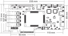
| Dimension | Carrier: 235mm x 111mm SOM: 80mm x 60mm |
| PCB | SOM: 12 Layer Carrier: 6 Layer Independent GND and Power Layers |
Quick Links
AX7Z035 Recommended by xilinx.com
Full documentation including DXF files will be provided by CodeRobin IT.


