Description
Zynq® UltraScale+™ MPSoC devices provide 64-bit processor scalability while combining real-time control with soft and hard engines for graphics, video, waveform, and packet processing.
Zynq UltraScale+ EGSource: https://www.xilinx.com/products/silicon-devices/soc/zynq-ultrascale-mpsoc.html
Broad Device Range for Next-Generation Applications:
- Quad Arm Cortex-A53
- Dual Arm Cortex-R5F
- 16nm FinFET+ Programmable Logic
- Arm Mali™-400MP2
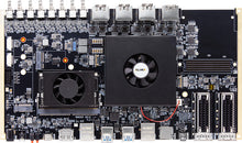
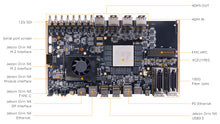
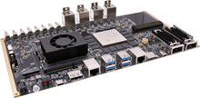
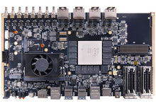
Z19-M is the first ALINX Heterogeneous Computing offering, with XCZU19EG FPGA + NVIDIA Jetson Orin NX module, rich ports including 12G-SDI, HPC FMC, 100G QSFP28+, and DP/HDMI. Built for 8K Video, ultra-low delay applications, 3D/Vision, AI, Machine Vision and Surgical System.
Z19-M is a single board design. For a SOM + Carrier Board combination, see our ACU19EG and Z19-P. For XCZU15EG board, have a look of our AXU15EG. For our Best selling all-rounder 7EV card, check for the Z7-P.
For a mid-range EG board, look for our AXU9EG; For an entry-level EG board, check out our AXU3EG
.FPGA Specification
| FPGA | XCZU19EG-2FFVC1760I |
| Processors | 4x ARM Cortex-A53, 1.333GHz 2x ARM Cortex-R5, 533MHz |
| GPU | ARM Mali-400 MP2, up to 667MHz |
| (PS) High-Speed Connectivity | PCIe® Gen2 x4, 2x USB3.0, SATA 3.1, DisplayPort, 4x Tri-mode Gigabit Ethernet |
| (PS) General Connectivity | 2x USB 2.0, 2x SD/SDIO, 2x UART, 2x CAN 2.0B, 2x I2C, 2x SPI, 4x 32b GPIO |
| Logic Cells (K) | 1,143 |
| CLB Flip-Flops(K) | 1,045 |
| CLB Look Up Tables (LUTs) (K) | 523 |
| Max. Distributed RAM (Mb) | 9.8 |
| Total Block RAM (Mb) | 34.6 |
| UltraRAM (Mb) | 36.0 |
| Clock Management Tiles (CMTs) | 11 |
| DSP Slices | 1,968 |
| PL PCIe Gen 3 | 3x Gen3x16 & 2x Gen3x8 |
| 100G Ethernet | 4x |
| 150G Interlaken | 4x |
| Transceivers | GTH 16.3Gb/s Transceivers: 32x GTY 32.75Gb/s Transceivers: 16x |
| 1.8V High-Performance (HP) I/Os | 416 |
| 3.3V High-Density (HD) I/O | 96 |
| Chip Level | Industrial Grade |
| Speed Grade | -2 |
| Working Temperature | -40℃~85℃ |
FPGA Features
| DDR4 | PS: 4x 2GB DDR4, total 8GB, 64bit Bus, Data Rate 2400Mbps PL: 8x 2GB DDR4, total 16GB, 64bit Bus, Data Rate 2400Mbps |
| QSPI FLASH | 2x 64MB, for system/boot, user data storage |
| eMMC FLASH | 32GB, for system/boot storage |
| SDI | 8x Two-way 12G-SDI, supports SD/HD/3G/6G/12G SDI rates, max 4K/60fps Input/Output |
| HDMI | 4x HDMI 2.1 Output, max 8K@60Hz 4x HDMI 2.1 Input, max 8K@60Hz with various formats |
| NVIDIA Orin Sockets | 1x PCIE3.0 x4 + 2x MIPI x4 Lane sockets |
| QSFP28 | 2x QSFP28 100G |
| FMC Expansion Port | 1x Standard HPC FMC Expansion Port, for Xilinx/ALINX or 3rd Party FMC cards. |
| UART | 1x PS via USB for serial communication with PC or devices 1x PS via FPC for serial screens |
| Ethernet Interface | PS: 1x 10/100/1000M Ethernet with RJ45 for data exchange |
| JTAG | 10-pin 2.54mm (0.1-inch) Pitch Standard JTAG port for FPGA Programs Debug and Download |
| SD Card Slot | 1 micro SD Card Slot, support SD Mode and SPI Mode |
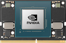
Nvidia Jetson ORIN NX Features
| Model | Jetson Orin NX 8GB | Jetson Orin NX 16GB |
| AI Performance | 70 TOPS | 100 TOPS |
| Ampere GPU | 1024 NVIDIA® CUDA® cores | 32 Tensor cores | |
| GPU Maximum Operating Frequency | 765 MHz | 918 MHz |
| Arm Cortex-A78AE CPU | Six-core Cortex A78AE Armv8.2 (64-bit) heterogeneous multi-processing (HMP) CPU | Eight-core Cortex A78AE Armv8.2 (64-bit) heterogeneous multi-processing (HMP) CPU |
| CPU Maximum Operating Frequency | 2 GHz | |
| Deep Learning Accelerator | 1x NVDLA, 20 TOPs (Sparse INT8) | 2x NVDLA, 20 TOPS each (Sparse INT8) |
| DLA Maximum Operating Frequency | 610 MHz | 614 MHz |
| Programmable Vision Accelerator (PVA) | 1x v2 | |
| Memory | 8 GB 128-bit LPDDR5 DRAM | 16 GB 128-bit LPDDR5 DRAM |
| Video Decode | Standards supported: H.265 (HEVC), H.264, VP9, AV1 - 1x8K30 (H.265) - 2x4K60 (H.265) - 4x4K30 (H.265) - 9x1080p60 (H.265) - 18x1080p30 (H.265) |
|
| Video Encode | Standards supported: H.265 (HEVC), H.264, AV1 - 1x4K60 (H.265) - 3x4K30 (H.265) - 6x1080p60 (H.265) - 12x1080p30 (H.265) |
|
| Power | 10W | 15W | 20W | 10W | 15W | 25W |
| M.2 | 1x PCIE (x2) Gen4 M.2, for ORIN storage | |
| M.2 | 1x M.2 Key-E, for WiFi/BT module, interface includes PCIEx1, USB2.0, UART, I2S and I2C signals. | |
| DP | 1x DisplayPort Output, for ORIN module, eDP 1.4, VESA DisplayPort 1.4a HBR3 | Maximum Pixel Clock at 1080 MHz: up to 7680x4320 at 30 Hz | |
| USB 3.0 | 4x, Type-A, supports HOST mode 1x, Type-C, supports HOST, SLAVE, OTG modes |
|
| Gigabit Ethernet | 1x, connects ORIN MDI output directly to the RJ45 | |
Power Supply
Voltage Input: +12 V DC, 2.1mm x 5.5mm
Current Input: Max. Current 5 A
What's Included
| FPGA Board | 1 | DC Fan (installed) | 1x FAN8080 |
| Mini USB Cable | 1 | Programming Cable | 1 set |
| 12V Power Adapter | 1 | Acrylic Panel (Top) | 1 |
| SD Card | 1x 32GB | SD Card Reader | 1 |
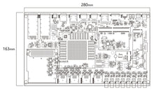
Dimensions
| Dimension | 280mm x 163mm |
| PCB | 18 Layer, Independent GND and Power Layers |
Resources & Downloads
Full documentation including Schematics, DXF files, Tutorials and more will be provided by CodeRobin IT.


