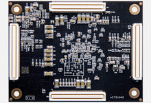
Description
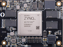
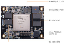
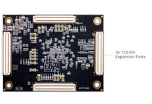
AC7Z100 is a Top-Range compact SOM based on Xilinx XC7Z100 Zynq-7000 SoC, equipped with DDR3 memory, QSPI Flash, eMMC, Clock sources, and Power. Through Four 120-pin I/O connectors on the backside, GTX Transceivers, PS side USB, Gigabit Ethernet, SD Card, and other MIO ports, JTAG, plus PL side IOs are exposed for Carrier board.
AX7Z100 Development Board takes the AC7Z100 SOM, a PCI Express card, with extensive ports including: SFP+, HDMI, Gigabit Ethernet, MIPI, SATA and USB. Perfect to use standalone, or as a reference board to speed up your design work.
AX7450 Development Board uses the same XC7Z100-2FFG900I SoC with FMC and PCI Express.
And our collections on the 2nd generation Zynq are well worth taking a look too.
Comparison
| Model | AC7Z035 | AC7Z100 |
| FPGA | XC7Z035-2FFG676I | XC7Z100-2FFG900I |
| Processor | ARM Cortex-A9 x2, Main Frequency 800MHz | |
| PL RAM | 1GB DDR3, Data Rate 1600Mbps | |
| PS RAM | 1GB DDR3, Data Rate 1066Mbps | |
| Speed Grade | -2 | |
| Chip Level | Industrial Grade | |
| Working Temperature | -40℃ to 85℃ | |
| 7 Series PL Equivalent | Kintex-7 | |
| Logic Cells | 275K | 444K |
| Look Up Tables (LUTs) | 171,900 | 277,400 |
| Flip-Flops | 343,800 | 554,800 |
| Total Block RAM | 17.6Mb | 26.5Mb |
| (# 36Kb Blocks) | (500) | (755) |
| DSP Slices | 900 | 2,020 |
| GTX Transceivers | 8-Channels1, Support PCIE Gen2.0 x8 | 16-Channels, Support PCIE Gen2.0 x8 |
| PS MIO | 37 | 37 |
| PL IO | 144 | 162 |
| Voltage Adjustable IOs | 96 | 96 |
| LVDS | 48 pairs | 48 pairs |
1 16x GTX Transceivers in SoC, GTX Quads 109 and 110 are not bonded out in FFG676 package, refer to UG865
SOM Features
| QSPI FLASH | 2x 256Mbit, for user data storage |
| eMMC FLASH | 8GB, for large capacity storage |
| AD Converter (XADC) | 2x 12-bit 1 MSPS ADCs with up to 17 Differential Inputs, on-chip Temperature and Voltage sensors |
| Crystal Oscillator | 33.333MHz provide PS Clock, 125 MHz for GTX Reference Clock, 200MHz for the PL Logic and DDR Reference |
| LEDs | 1 Power Indicator (PWR), 1 DONE, 1 User |
| Expansion Ports | 4x 120-pin Panasonic Industrial Grade Connectors (AXK5A2137YG), matching connector on the carrier board is AXK6A2337YG |
Power Supply
Voltage Input: +5 V DC
What's Included
FPGA SOM: 1
Dimensions
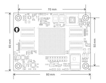
| Size | 80mm x 60mm x 10.8mm | Connector Height | 3.0mm |
| PCB | 12-Layer |
Resources & Downloads
AC7Z100 Recommended by xilinx.com
Full documentation including Schematics, Demo projects (if applicable) will be provided by CodeRobin.
Revision History
| Date | Revision | Model Name | Notes |
| 03 | AC7Z100C | Current | |
| 02 | AC7Z100B | - | |
| 01 | AC7Z100 | First production release |


