Description
The Versal AI Edge series delivers high performance, low latency AI inference for intelligence in automated driving, predictive factory and healthcare systems, multi-mission payloads in aerospace & defense, and a breadth of other applications. More than just AI, the Versal AI Edge series accelerates the whole application from sensor to AI to real-time control, all while meeting critical safety and security requirements such as ISO 26262 and IEC 61508.Source: https://www.amd.com/en/products/adaptive-socs-and-fpgas/versal/ai-edge-series.html
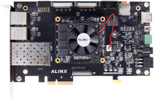
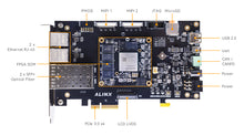
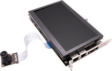
VD100 is ALINX's first Versal AI Edge offering to date, PCIe3.0 x4 Card with VE2302 FPGA, 2x SFP+, 2x MIPI, 1x LCD LVDS, and CAN/CAN FD, offers AIE-ML and DSP hardware acceleration engines. Ideal for ADAS/Automated Drive, Collaborative Robotics, UAV & Multi-Mission Payloads and Ultrasound Imaging.
Ideal for:
- AI Edge Box
- Edge Sensor (e.g., radar, LiDAR, vision)
- Converged Networking
- Medical Imaging Devices
- Data and Signal Processing Systems
The SOM model is V100.
Model Specification
| SOM Model | V100 |
| FPGA | XCVE2302-SFVA784-1LP-E-S |
| Chip Level | Commercial Grade |
| Speed Grade | -1 |
| Working Temperature | 0℃ ~ 100℃ |
| AI Engine-ML Tiles | 34 |
| AI Engine Tiles | 0 |
| AIE/AIE-ML Data Memory (Mb) | 17 |
| AIE-ML Shared Memory (Mb) | 68 |
| System Logic Cells | 328,720 |
| LUTs | 150,272 |
| DSP Engines | 464 |
| NoC Master / NoC Slave Ports | 5 |
| Distributed RAM (Mb) | 4.6 |
| Total Block RAM (Mb) | 5.4 |
| UltraRAM (Mb) | 43.6 |
| Accelerator RAM (Mb) | 32 |
| Total PL Memory (Mb) | 85.6 |
| DDR Memory Controllers | 1 |
| DDR Bus Width | 64 |
| Application Processing Unit | Dual-core Arm® Cortex-A72 |
| Real-Time Processing Unit | Dual-core Arm Cortex-R5F |
| PS Connectivity | Ethernet (x2); UART (x2); CAN-FD (x2); USB 2.0 (x1); SPI (x2); I2C (x2) |
| GTYP Transceivers | 8 |
| PCI Express® | 1 x Gen4x8 |
| 40G Multirate Ethernet MAC | 1 |
Features
| DDR4 | 4x 1GB DDR4, total 4GB, 64bit Bus, Data Rate 3200Mbps |
| QSPI FLASH | 2x 256Mbit, for user data storage |
| eMMC FLASH | 8GB, for system/boot storage |
| PCI Express | PCI Express 3.0 x4 lane |
| SFP+ | 2x SFP+ Interfaces, speed of each channel up to 12.5Gb/s |
| MIPI | 2x MIPI x4 Lane, for camera e.g. ALINX AN5020 |
| LVDS | 1x LVDS, for display e.g. ALINX AN7000 |
| CAN / CAN FD | 1x, 3-pin connector |
| PMOD | 1x 12-pin 2.54mm pitch connector, Includes: 2x 3.3V, 2x GND, 8x 3.3V I/O. |
| USB 2.0 | 1x USB2.0, for external USB devices |
| USB UART | 2x, for serial communication with PC or devices |
| Ethernet Interface | 1x 10/100/1000M Ethernet with RJ45 for data exchange |
| Oscillator | 1x 32.768KHz for PS RTC 1x Single-ended 33.333MHz provide PS Clock 1x Differential 200MHz for the PL Logic and DDR Reference |
| JTAG | 10-pin 2.54mm (0.1-inch) Standard JTAG port for Programs Debug and Download |
| Temperature Sensor | LM75, for onboard ambient temperature |
| EEPROM | EEPROM 24LC04 with IIC |
| SD Card Slot | 1 micro SD Card Slot, support SD Mode and SPI Mode |
| Real Time Clock | 1x Battery Holder |
| LEDs | SOM: 1 Power Indicator (PWR), 1 DONE Carrier: 1 PWR, 1 PS User, 1 PL User |
| Push-Buttons | 1 PS User, 1 PL User |
Power Supply
Voltage Input: +12 V DC, 2.1mm x 5.5mm
Current Input: Max. Current 3 A
What's Included
| FPGA Board | 1 | DC Fan (installed) | 1 |
| Mini USB Cable | 1 | Programming Cable | 1 set |
| 12V Power Adapter | 1 | PCI Fence | 1 |
| SD Card | 1x 32GB | SD Card Reader | 1 |
Dimensions
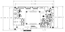
| Dimension | 181.71mm x 106.65mm (Carrier Board) 65mm x 60mm (SOM) |
| PCB | 8 Layer (Carrier Board) 16 Layer (SOM) Independent GND and Power Layers |
Resources & Downloads
VD100 Recommended by xilinx.com
Full documentation including: Tutorial with source code; Reference Design, CAD/DXF, Schematic PDF; and much more, will be provided by CodeRobin.


