Description
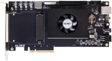
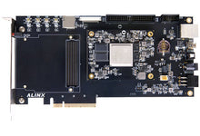
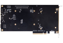
AXKU5 is a High Performance PCIE3.0 x8 Card with XCKU5P FPGA, 1x HPC FMC, 1x MIPI, enabling high signal processing bandwidth, rich expandability. Ideal for packet processing and DSP-intensive functions, wireless MIMO, PON, and Nx100G.
The SOM model used is ACKU5.
FPGA Specification
| Model | AXKU3 | AXKU5 |
| SOM | ACKU3 | ACKU5 |
| FPGA | XCKU3P-2FFVB676I | XCKU5P-2FFVB676I |
| Speed Grade | -2 | -2 |
| Chip Level | Industrial Grade | Industrial Grade |
| Working Temperature | -40℃~85℃ | -40℃~85℃ |
| System Logic Cells (K) | 356 | 475 |
| CLB Flip-Flops (K) | 325 | 434 |
| CLB LUTs (K) | 163 | 217 |
| Max. Distributed RAM (Mb) | 4.7 | 6.1 |
| Total Block RAM (Mb) | 12.7 | 16.9 |
| UltraRAM (Mb) | 13.5 | 18.0 |
| Clock Mgmt Tiles (CMTs) | 4 | 4 |
| DSP Slices | 1,368 | 1,824 |
| PCIE4 (PCIe® Gen3 x16) | 1 | 1 |
| 100G Ethernet w/ KR4 RS-FEC | 0 | 1 |
| GTY Transceiver | 28Gb/s x16 | 28Gb/s x16 |
| HD I/O | 72 | 72 |
| HP I/O | 96 | 96 |
| LVDS Pairs | 45 | 45 |
Board Features
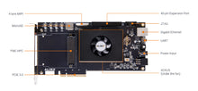
| DDR4 | 2 Pieces of 1G DDR4, 2GB total, 32 bit bus width, up to 2666Mbps |
| QSPI Flash | 2 Pieces of 32MB, for FPGA bin file or user data storage |
| FMC | 1x HPC (*) |
| PCI Express 3.0 | x8 lane, for communication with PC |
| MIPI | 1x MIPI x4 Lane, rate up to 2.5Gb/s |
| USB UART | for Serial Communication with PC/Devices |
| Gigabit Ethernet | 1x 10/100/1000M Ethernet with RJ-45 |
| Crystal Oscillator | (SOM) 2x 200MHz Differential Crystal, Reference Clock for the DDR4 and FPGA |
| JTAG | 10-pin 2.54mm (0.1-inch) Standard JTAG port for Program Debug and Download |
| 40-pin Expansion Port | 1x 40-pin Expansion Port (2.54mm / 0.1 inch pitch), fit with ALINX Binocular Camera Module, TFT LCD Screen, Camera, AD/DA, etc. Includes: 1x 5V, 2x 3.3V, 3x GND, 34x I/O. |
| Temperature Sensor | LM75A, for onboard ambient temperature |
| RTC | onboard RTC with battery holder (1x CR1220) |
| EEPROM | 1x 24LC04 with IIC |
| SD Card Slot | 1 micro SD Card Slot, support SD Mode and SPI Mode |
| LED | SOM: 1 PWR, 1 DONE, 1 User; Carrier: 8 LEDs, 4 User, 2 UART (TX/RX), 2 User (on PCI Bracket) |
| Push-Buttons | 5x: 1 On/Off, 4 User |
Power Supply
Voltage Input: +12 V DC, Barrel plug 2.1 x 5.5mm
Current Input: Max. Current 3 A
What's Included
| FPGA Board | 1 | DC Fan (installed) | 1 |
| Mini USB Cable | 1 | Programming Cable | 1 set |
| 12V Power Adapter | 1 |
Dimensions
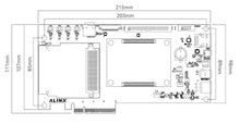
| Dimension | 215mm x 111mm (Carrier Board) 80mm x 60mm (SOM) |
| PCB | 10 Layer (Carrier Board) 14 Layer (SOM) Independent GND and Power Layers |
Resources & Downloads
AXKU5 Recommended by xilinx.com
Full documentation including Schematics, Demo projects (if applicable) will be provided by CodeRobin.


