Description
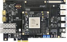
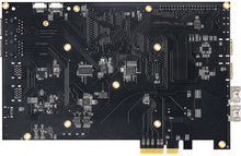
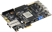
PZ-ZU7EV-KFB is an Xilinx Zynq UltraScale+ MPSoC XCZU7EV FPGA Development Board. Equipped with 2x 10G SFP+, 1x HPC FMC, M.2 NVMe, 2x SATA, DisplayPort and rich I/O ports, built for Packet Processing and Communication. Ideal for 5G Wireless, Next-generation ADAS, Multimedia, AI, Machine Learning and Embedded Vision.
Design Highlights:
- IO Voltage 1.8/2.5/3.3 Adjustable
- Dual QSPI Flash for faster booting
- CAN, RS485, MIPI, HDMI
The SOM used on this development board is PZ-ZU7EV-SOM.
FPGA Specification
| SOM Model | PZ-ZU7EV-SOM |
| FPGA | XCZU7EV-2FFVC1156I |
| Processors | 4x ARM Cortex-A53, up to 1.5GHz 2x ARM Cortex-R5, up to 600MHz |
| GPU | ARM Mali-400 MP2, up to 667MHz |
| System Logic Cells (K) | 504 |
| CLB Flip-Flops (K) | 461 |
| CLB LUTs (K) | 230 |
| Max. Distributed RAM (Mb) | 6.2 |
| Total Block RAM (Mb) | 11.0 |
| UltraRAM (Mb) | 27.0 |
| Clock Management Tiles (CMTs) | 8 |
| DSP Slices | 1,728 |
| Video Codec Unit (VCU) | 1 |
| AMS - System Monitor | 1 |
| GTH 16.3Gb/s Transceivers | 24 |
| PS to PL Interface | 12 x 32/64/128b AXI Ports |
| (PS) High-Speed Connectivity | PCIe® Gen2 x4, 2x USB3.0, SATA 3.1, DisplayPort, 4x Tri-mode Gigabit Ethernet |
| (PS) General Connectivity | 2xUSB 2.0, 2x SD/SDIO, 2x UART, 2x CAN 2.0B, 2x I2C, 2x SPI, 4x 32b GPIO |
| Chip Level | Industrial Grade |
| Speed Grade | -2 |
| Working Temperature | -40℃ ~ +85℃ |
Board Features
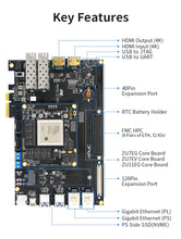
| DDR4 | PS: 4x 1GB DDR4, total 4GB, 64bit Bus, Data Rate 2400Mbps PL: 4x 1GB DDR4, total 4GB, 64bit Bus, Data Rate 2400Mbps |
| eMMC FLASH | 8GB, for system/boot storage |
| QSPI FLASH | 2x 32MB, for user data storage |
| EEPROM | 64Kb |
| Boot Mode | JTAG/SD/QSPI/EMMC |
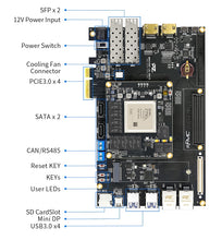
| USB UART | 1x, for serial communication with PC or devices |
| RS485 | 1x RS485 interface |
| CAN | 1x CAN interface |
| SD Card Slot | 1 micro SD Card Slot, support SD Mode and SPI Mode |
| Gigabit Ethernet | 1x PS, 1x PL |
| USB 3.0 | 4x USB3.0, for external USB devices |
| JTAG | via USB |
| DP | 1x Mini DisplayPort Output, Supports 4K@30Hz or 1080P@60Hz |
| HDMI (4K) | 1x Input, 1x Output |
| M.2 | 1x NVME M.2, for M.2 SSD storage |
| SFP+ | 2x SFP+ Interfaces, speed of each channel up to 12.5Gb/s |
| SATA | 2x SATA, for external HD Storage |
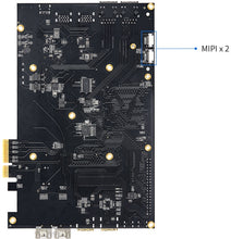
| MIPI | 2x MIPI |
| FMC | 1x HPC (DP, HA, HB, LA) |
| PCI Express | PCIe Gen3 x4, each channel up to 8GBaud |
| 40-pin Expansion Port | 2x 40-pin Expansion Port (2.54mm / 0.1 inch pitch), fit with Binocular Camera Module, TFT LCD Screen, Camera, AD/DA, etc. Includes: 1x 5V, 1x 3.3V, 6x GND, 32x I/O. |
| 120-pin Expansion Port | 1x High-Speed |
| Active Crystal Oscillator |
1x Single-ended 33.333MHz provide PS Clock 1x Differential 125MHz for the GTX 1x Differential 200MHz for the FPGA Logic |
| LEDs | 3x SOM, 2x Carrier |
| Push Buttons | 1x RESET (SOM), 1x Power On/Off, 2x User |
| Board-to-Board connectors | 3x 168-pin 0.5 mm Pitch Hirose Industrial Grade Connectors (FX10A-168S-SV), matching connector on the SOM is FX10A-168P-SV |
Power Supply
Voltage Input: +12 V DC, 2.5mm x 5.5mm
Current Input: Max. Current 3 A
What's Included
| FPGA Board | 1 | Heat Sink & DC Fan (installed) | 1x |
| 12V DC Power Adaptor | 1x | Micro-USB Cable | 2x |
| SD Card | 1x 8GB | SD Card Reader | 1x USB |
Dimensions
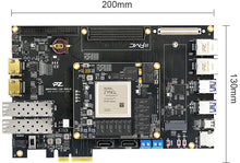
| Dimension | 200.00mm x 130.00mm |
| PCB | Immersion gold (Au) PCB, Independent GND and Power Layers |
Resources & Downloads
PZ-ZU7EV-KFB User Manual (Coming soon)
Full documentation including: Tutorial with source code; Reference Design, CAD/DXF, Schematic PDF; and much more, will be provided by CodeRobin.


