Description
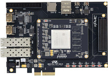
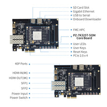
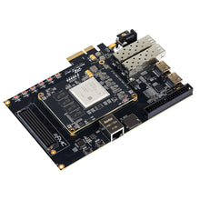
PZ-K7325T-FH is an Xilinx Kintex-7 XC7K325T Mid-range FPGA Development Board. Equipped with 2GB DDR3 memory, QSPI Flash, Clock sources on the PZ-K7325T SOM; 2x HDMI (4K), 2x SFP+, and 1x HPC FMC on the PCIE form Carrier board, gives you a versatile cost-effective kit for fast developing your mission critical applications.
Design Highlights:
- Fully connected HPC FMC (DP, HA, HB, LA)
- SFP+, PCIE 2.0, HDMI(4K)
- IO Voltage 1.8/2.5/3.3 Adjustable
- 5x User LED, 5x User Push button
The SOM used on this development board is PZ-K7325T.
FPGA Specification
| FPGA | XC7K325T-2FFG900I |
| Slices | 50,950 |
| Logic Cells | 326,080 |
| CLB Flip-Flops | 407,600 |
| Maximum Distributed RAM (Kb) | 4,000 |
| Block RAM/FIFO w/ ECC (36 Kb each) | 445 |
| Total Block RAM (Kb) | 16,020 |
| CMTs (1 MMCM + 1 PLL) | 10 |
| Maximum Single-Ended I/O | 500 |
| Maximum Differential I/O Pairs | 240 |
| DSP48 Slices | 840 |
| PCIe® Gen2 | 1 |
| Analog Mixed Signal (AMS) / XADC | 1 |
| GTX Transceivers (12.5 Gb/s Max Rate) | 16 |
| Chip Level | Industrial Grade |
| Speed Grade | -2 |
| Working Temperature | -40℃ ~ +85℃ |
Board Features
| RAM | DDR3, 2GB, 4x 512MB, 64bit Bus |
| QSPI FLASH | 32MB, for user data storage |
| EEPROM | 1x AT24C64D-SSHM-T |
| Boot Mode | JTAG/QSPI |
| HDMI Input | TI TMDS181RGZR |
| HDMI Output | TI SN75DP159RGZ |
| SFP+ | 2x SFP+ Interfaces, speed of each channel up to 10Gb/s |
| Gigabit Ethernet | 1x RJ45 |
| JTAG | 1x built-in, via USB |
| UART | 1x, for serial communication with PC or devices |
| 40-pin Expansion Port | 1x, 2.54mm-pitch, 32 Single-Ended or 16 Pairs Differential IO |
| Active Crystal Oscillator (SOM) |
1x Differential 125MHz for the GTX 1x Differential 200MHz for the FPGA Logic |
| SD Card Slot | 1x micro-SD Card Slot, support SD mode and SPI mode |
| LEDs | SOM: 1x DONE, 5x USER Carrier: 1x POWER, 5x USER |
| Push Buttons | 1x RESET, 5x USER |
| PCIe 2.0 | x4 wide, x2 Lane, up to 5.0 GT/s per Lane |
| FMC | 1x HPC (DP, HA, HB, LA) |
| Board-to-Board connectors | 4x 120-pin 0.6 mm Pitch Hirose Industrial Grade Connectors (FX8-120S-SV), matching connector on the SOM board is FX8-120P-SV |
Power Supply
Voltage Input: +12V, via DC or PCIE
Max 3A
What's Included
| FPGA Board | 1 | Heat Sink & DC Fan (installed) | 1x |
| 12V DC Power Adaptor | 1x | Micro-USB Cable | 2x |
| SD Card | 1x 8GB | SD Card Reader | 1x USB |
Dimensions
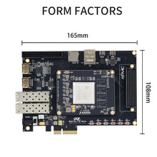
| Dimension | 165.00mm x 108.00mm |
| Connector Mated height | 3.0mm |
| PCB | Immersion gold (Au) PCB, Independent GND and Power Layers |
Documents & Quick Links
Coming soon
Full documentation including DXF files will be provided by CodeRobin IT.


