Description
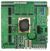
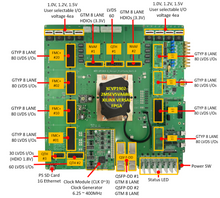
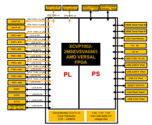
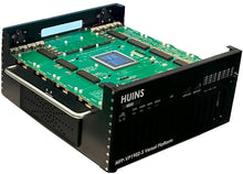
HUINS MFP-VP1902-S is a VERSAL PREMIUM XCVP1902 single FPGA Board for SoC/ASIC Design RTL H/W System-Level Verification, Rapid Prototyping, S/W Testing and Development. With 18.5 Million logic cells and total 2,000 I/Os. 8x FMC+, 3x QTH, 2x NVAF, 2x QSFP-DD. Carefully designed for maximum performance, with respect to signal integrity, speed and other critical issues.
As ASIC and SoC design complexity increases rapidly due to the rapid evolution of AI and Machine Learning-based chips, extensive validation of silicon and software prior to tape-out is essential. To meet these requirements, Huins seeks to provide the best, most efficient boards with proven FPGA technology and know-how that are recognized as the best in the industry.
The VP1902 has 2.2x more logic cells compared to the previous generation VU19P FPGA, reaching 18.5 million logic cells. Delivering maximum capacity and connectivity with rammable logic density and 2.4x higher I/O bandwidth, the VP1902 adaptive SoC leverages a universal architecture including programmable network-on-chip to outperform previous generations. Delivers up to 8.5x faster debugging performance compared to VU19P FPGAs.
MFP-VP1902-S can be easily expanded with various functions through FMC+ Supports 3200MHz and 32GB memory.
It is possible to manufacture and verify desired expansion modules such as PCIe Gen5, CSI, DSI, USB3.0, DDR4, Ethernet, HDMI, VX1, etc., and remote download and control of Power/Reset/Config control is possible through USB.
Low skew, high-speed clocks are distributed by the clock buffer. The clock can use the clock output of the board's 4 oscillators.
FPGA Specification
| VERSAL PREMIUM VP1902 ADAPTIVE SOC | ||
|---|---|---|
| Adaptable Engines | System Logic Cells (K) | 18,507 |
| LUTs (K) | 8,460 | |
| Intelligent Engines | DSP Engines | 6,864 (DSP58) |
| Scalar Engines | Application Processing Unit | Dual-Core Arm® Cortex®-A72 |
| Real-Time Processing Unit | Dual-Core Arm Cortex-R5F | |
| Memory | Hardened DDR Memory Controllers | 14 |
| Block RAM (Mb) | 239 | |
| UltraRAM (Mb) | 619 | |
| Transceivers | GTYP Transceivers (32.75 Gbps) | Up to 128 |
| GTM Transceivers (58G (112G)) | 32 (16) | |
| Hardened IP | 100G Multirate Ethernet MAC | 12 |
| 600G Ethernet MAC | 4 | |
| PCI Express® | 16 x Gen5 x 4 | |
| Packaging | XPIO (Fabric Facing) | Up to 264 DDR-only, 2064 DDR + PL |
| HDIO | 88 | |
| Footprint | 77.5 x 77.5 mm | |
Features
| FPGA | |
|---|---|
|
VERSAL PREMIUM XCVP1902-2MSEVSVA6865 |
|
| MEMORY | |
| SODIMM 2EA | DDR4 SODIMM x 2EA, Max. 3200MHz, 32GB x 2EA |
| High-Speed I/O | |
| QSFP-DD “0” | GTM 8 LANE, 400G Optic Module |
| QSFP-DD “1” | GTM 8 LANE, 400G Optic Module |
| FMC+ “01” | GTYP 8 LANE + 80 LVDS I/Os (XIO 1.5V), PCIE GEN5 Support |
| FMC+ “10” | GTYP 8 LANE + 80 LVDS I/Os (XIO 1.5V), PCIE GEN5 Support |
| FMC+ “02” | GTYP 8 LANE + 80 LVDS I/Os (XIO 1.5V), PCIE GEN5 Support |
| FMC+ “20” | GTYP 8 LANE + 80 LVDS I/Os (XIO 1.5V), PCIE GEN5 Support |
| FMC+ “03” | GTYP 8 LANE + 80 LVDS I/Os (XIO 1.5V), PCIE GEN5 Support |
| FMC+ “30” | GTYP 8 LANE + 80 LVDS I/Os (XIO 1.5V), PCIE GEN5 Support |
| FMC+ “04” | GTYP 8 LANE + 80 LVDS I/Os (XIO 1.5V), PCIE GEN5 Support |
| FMC+ “40” | GTYP 8 LANE + 80 LVDS I/Os (XIO 1.5V), PCIE GEN5 Support |
| NVAF “1” | GTM 8 LANE, HDIOs (3.3V) |
| NVAF “2” | GTM 8 LANE, HDIOs (3.3V) |
| QTH “1” | 60 LVDS I/Os (XIO 1.5V) |
| QTH “2” | 60 LVDS I/Os (XIO 1.5V) |
| QTH “3” | 30 LVDS I/Os (HDIO 1.8V) |
| Peripheral | |
| JTAG | USB JTAG 1Port, USB C-type |
| UART | USB UART 2Port, USB C-type |
| SD Card | SD 3.0 1Port, 32GB, uSD 3.0 |
| USB | USB 2.0 1Port, Host, USB C-type |
| QSPI Flash Memory | QSPI Flash Memory 128GB x 2EA |
| Gigabit Ethernet | 10/100/1000 Base-TX 1Port, Modular Jack |
| User SWs | DIP SW (4EA), Push Button SW (3EA) |
| User LEDs | LEDs (12EA) |
| Clock | |
| Global Clock | Clock Module (CLK 0~3) Clock Generator 6.25 ~ 400MHz |
| Connector I/O Power | |
| Voltage Regulator | FMC+ #1, #2, #3, #4, #5, #6, #7, #8 : 1V, 1.2V, 1.5V select QTH #1, #2 :1.5V #3 : 1.8V |
| Power | |
| AXT Power 1500W | 24Pin ATX Power Connector 1ea 8Pin 12V Aux. Power Connector 2ea |
| FAN + Cooler | |
| Cooler | FPGA : Active Air Cooler, Case : FAN 4ea |
| Borad Size | |
| PCB | 355 mm (W) x 369 mm (D) x 3mm (T), 36 Layer |
| Case | |
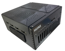
| Case | 374 mm (W) x 360 mm (D) x 153.6 mm (H) |
Resources & Downloads
MFP-VP1902-S User Manual (PDF)
High-Res Images
Full documentation including User Manual, Pin Out List, Schematics (in searchable .pdf format) will be provided by CodeRobin IT.


