Description
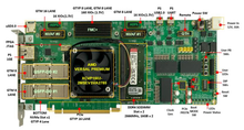
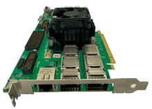
HUINS MFP-VP1502-PCIe is a VERSAL PREMIUM XCVP1502 single FPGA Board for SoC/ASIC Design RTL H/W System-Level Verification, Rapid Prototyping, S/W Testing and Development. PCIe Gen5 support enables 2x faster speed than Gen4. With 3.7 Million Logic Cells and abundant high speed transceivers and I/Os. 2x NVAF, 2x ADF6, 2x QSFP-DD, 1x FMC+, 1x NVMe. Designed to provide maximum performance for data center and edge computing development.
As ASIC and SoC design complexity increases rapidly due to the rapid evolution of AI and Machine Learning-based chips, extensive validation of silicon and software prior to tape-out is essential. To meet these requirements, Huins seeks to provide the best, most efficient boards with proven FPGA technology and know-how that are recognized as the best in the industry.
MFP-VP1502-PCIe can be easily expanded with various functions through FMC+.
FPGA Specification
| VERSAL PREMIUM VP1502 ADAPTIVE SOC | ||
|---|---|---|
| Programmable Logic | System Logic Cells (K) | 3,763 |
| LUTs | 1,720,448 | |
| DSP Engines | 7,440 | |
| Processing System | Application Processing Unit | Dual-Core Arm® Cortex®-A72 |
| Real-Time Processing Unit | Dual-Core Arm Cortex-R5F | |
| Memory | DDR Memory Controllers | 4 |
| Block RAM (Mb) | 89 | |
| UltraRAM (Mb) | 366 | |
| Transceivers | GTYP Transceivers (32.75 Gbps) | Up to 28 |
| GTM Transceivers (58G (112G)) | 60 (30) | |
| Integrated Protocol IP | PCIe w/DMA (CPM5) | 2 x Gen5x8 |
| PCI Express® | 2 x Gen5x4 | |
| 100G Multirate Ethernet MAC | 4 | |
| 600G Ethernet MAC | 3 | |
| 400G High-Speed Crypto Engine | 2 | |
| Packaging | XPIO DDR Only, XPIO DDR+PL, XPIO PL Only, HDIO, MIO | 132, 516, 54, 0, 78 |
| Package Dimensions (mm) | 50 x 50 | |
Features
| FPGA | |
|---|---|
|
VERSAL PREMIUM XCVP1502-2MSEVSVA2785 |
|
| MEMORY | |
| SODIMM 2EA | DDR4 SODIMM x 2EA, Max. 3200MHz, 32GB x 2EA |
| High-Speed I/O | |
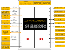
| PCIe Edge | Gen5 x8 or Gen4 x16 lane connected to PCIe Hard IP(CPM5) |
| QSFP-DD "0" | GTM 8 LANE x 56G, 400G Optic Module |
| QSFP-DD "1" | GTM 8 LANE x 56G, 400G Optic Module |
| FMC+ "01" | GTM 8 LANE + GTYP 8 LANE + 160 I/Os (XIO 1.5V) |
| NVAF "1" | GTM 16 LANE |
| NVAF "2" | GTM 16 LANE |
| ADF6 "1" | 16 I/Os(XIO 1.5V), I2C x2, 12V, 3.3V, 1.5V |
| ADF6 "2" | 16 I/Os(XIO 1.5V), I2C x2, 12V, 3.3V, 1.5V |
| NVMe | GTYP 4 LANE |
| PS Peripheral | |
| JTAG | JTAG 1 Port, 14-pin |
| UART | USB UART 2 Port, USB C-type |
| SD Card | SD 3.0 1 Port, 32GB |
| USB | USB 2.0 1 Port, Host, USB C-type |
| QSPI Flash Memory | QSPI Flash Memory 1Gb x 2EA |
| Gigabit Ethernet | 10/100/1000 Base-TX 1 Port, Modular Jack |
| User SWs | DIP SW (8EA), Push Button SW (3EA) |
| User Pin Header | XIO (16EA), MIO (10EA) |
| User LEDs | LEDs (12EA) |
| Clock | |
| Clock | Si5341 x1: 100Hz ~ 712.5MHz 83PN156DKILF : 100,125,150,156.25MHz |
| Power | |
| 12V 6Pin connectors, no power draw from PCIe pins. | |
| FAN + Cooler | |
| Cooler | FPGA : Active Air Cooler |
| Borad Size | |
| PCB | 120 mm x 280 mm, 22 Layer |
Resources & Downloads
High-Res Images
Full documentation including User Manual, Pin Out List, Schematics (in searchable .pdf format), Reference Designs/Demos will be provided by CodeRobin IT.


